Analog in-memory AI · Sovereign SATCOM silicon

We compute AI in analog memory.

A GPU spends most of its power moving data to compute. We delete the movement: antenna signals enter as voltages, conductances do the multiplication, currents sum themselves — 65,536 operations in one physical event, no clock, no data movement. That's how a beamforming supercomputer fits on a satellite's power budget.

Why analog

A GPU moves data to compute. We compute where the data already is.

Digital accelerators spend almost all their energy shuttling weights back and forth between memory and arithmetic units. In orbit — where you have watts, not kilowatts — that overhead is fatal. Analog in-memory computing deletes the movement entirely: the weight never leaves the cell, because the cell does the math.

Digital accelerator

Compute, then move, then repeat

  • Weights stream from memory every cycle — the bottleneck is the bus, not the math
  • Energy scales with data moved; most of the power budget never touches a multiply
  • Radiation tolerance bolted on afterward, at the cost of area and power
AresSemi analog IMC

The memory is the multiplier

  • Weights live as conductance and never move — the multiply happens in place
  • 65,536 MACs per tile in one read: 15–25 TOPS/W, several × a rad-tolerant FPGA
  • The weight is atoms, not charge — radiation hardness is inherent, not added
The principle

Three laws of physics, one operation.

The weights of a neural network are stored as the electrical conductance of nanoscale ReRAM cells. From there, the arithmetic is just what the devices already do.

OHM'S LAW

The cell multiplies

Drive a cell of conductance G with a voltage V and the current I = G·V is already the product — one multiplication, one device, no logic.

KIRCHHOFF

The column sums

Tie 256 cells to one wire and the currents add themselves. A 256×256 tile is 65,536 multiply-accumulates in a single physical event.

GEOMETRY

The state is atoms

A weight is the shape of a conductive filament a few nanometers wide — not stored charge. A particle strike has nothing to flip.

Realistic 3D render of one 1T1R cell as built: M4 bit line, TiN top electrode, HfO₂ switching layer, BEVA, the Cu via ladder, HKMG access NMOS and p-Si substrate, with the conductive filament detailed inside the switching layer
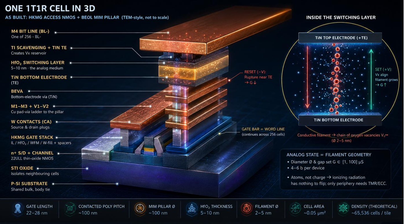
One 1T1R cell, as built — the conductive filament inside the HfO₂ is the weight
The architecture

The crossbar is the processor.

Wire 256 of these cells into a row and 256 into a column, and the grid computes a full 256×256 matrix-vector multiply in a single read. There is no separate compute unit — the memory array itself is the arithmetic. Antenna voltages go in along the rows; the beamformed currents come out along the columns. 65,536 multiply-accumulates, one physical event, no clock.

Analog crossbar · 6×6 of 256×256 computing
Ij = Σ Gij · Vi  ·  Ohm multiplies, Kirchhoff sums — the matrix multiply is the wiring
The product family

One architecture, three generations.

The same analog tile — a 256×256 ReRAM crossbar — qualified on a single mask-set family, so each generation inherits the last one's evidence and scales the array.

Gen-1 single 256x256 ReRAM tile block diagram with dimensions
Demonstrator

Gen-1

A single 256×256 tile — crossbar, PWM drivers, column ADC strip and calibration — that proves the cell in real silicon.

Tile
0.44 × 0.57 mm
Compute
0 MACs / read
Raw
1.3–3.9 TOPS
Node
TSMC 22ULL + eRRAM
MPW silicon · 2026–27
Gen-2 8x8 die floorplan with dimensions and area budget
LEO payload

Gen-2 · 8×8

A 32-chain beamforming engine: 64 squint-free beams in ~3 W on a ~58 mm² die, built for an in-orbit demonstration.

Die
~7.2 × 8.0 mm · 58 mm²
Beams
64 · squint-free
Raw
~85–250 TOPS
Power
~3 W
Tape-out 2029–30 · LEO IOD ~2030
FLAGSHIPB+ 16x16 die floorplan with dimensions, tile zoom and area budget
VHTS flagship

B+ · 16×16

The full payload chip: 64 beams across a 2 GHz window at ~13 TOPS, 15–25 TOPS/W on a 156 mm² die. GEO and IRIS²-class.

Die
12.2 × 12.8 mm · 156 mm²
Raw
336–1000 TOPS
Delivered
~13 TOPS @ 10–12 W
Efficiency
15–25 TOPS/W
Flagship tape-out · 2030–32
B+ · Flagship render AresSemi B+ 16×16 VHTS flagship — die with the 16×16 ReRAM tile array exploded above its FC-BGA package and C4 bump field

The B+ 16×16 — 256-tile die above its flip-chip FC-BGA package · render, illustrative geometry

Raw analog throughput · B+
0TOPS in 156 mm² · up to ~1 PetaOP/s

256 analog tiles, each 65,536 multiply-accumulates per read — that's the raw ceiling. We deliver ~13 TOPS to the beamforming workload at just 10–12 W, and the gap isn't lost compute: it's compute we never spend.

0
MACs per tile-read
0 tiles
on one 156 mm² die
15–25 TOPS/W
vs 2–5 for a rad-tol FPGA
Raw is the ceiling. Delivered is what the mission needs — the difference is energy we don't burn.
01

We compute only what matters

Beamforming weight matrices are sparse. The chip evaluates the products that form the beams and nulls — not all 65,536 cells in every tile, every cycle. Less arithmetic by design, not by limitation.

02

Idle tiles burn nothing

Tiles not in use are power-gated. A GPU draws near-full power even at 20% utilization; here, unused compute costs zero watts — which is exactly why the efficiency reaches 15–25 TOPS/W.

03

Read at the signal's pace

The raw ceiling assumes a 30 MHz readout. The sub-band math only needs ~10 MHz, so we run the converters where the signal lives — racing them faster would spend power for no useful output.

Every AI chip has this gap — a GPU marketed at “1000 TOPS” delivers a fraction in any real workload. The difference is that our unused compute draws no power. The low delivered figure isn't a weakness; it's the proof of the efficiency.
The shift

We replace an entire digital beamforming system with the real power of analog-AI computing.

A conventional payload needs racks of phase shifters and DSPs to form and steer its beams. On the B+, that whole subsystem collapses into one 156 mm² die — because beamforming isn't a processing stage bolted on, it is the chip. Here's how it works.

Digital beamforming

One array. Many beams at once.

A phased array isn't limited to a single beam. By applying several weight sets to the same antenna data in parallel, the chip forms independent beams pointing at different users simultaneously — each one a separate matrix-vector multiply, all computed in the same analog read. This is how a single payload serves dozens of spot beams across its coverage. Digital beamforming, delivered by true analog-AI power.

Beam pattern · 16 simultaneous beams forming
What analog unlocks

Anti-jam becomes native hardware.

Because a beam is a matrix-vector multiply and a null is the same multiply with different weights, steering 64 beams and nulling every interferer happens in one analog read — squint-free across the full 2 GHz window, with nulls that stay deep where phase-only systems collapse. Adaptive MVDR nulling stops being the expensive part of the payload.

The same crossbar that makes the chip efficient makes it jam-resilient. Performance and protection come from the same physics.

Beam pattern · 1 user · 2 jammers MVDR live
Beam hopping

One beam, everywhere it's needed.

Traffic in orbit is bursty — a cell that's busy now is idle a moment later. Instead of lighting every cell continuously, a hopping beam dwells where the demand is and jumps to the next cell in microseconds, following the traffic. The dwell schedule is just another weight pattern, so the beam re-points with no settling time and no moving parts — capacity goes where it's needed, instant by instant.

Coverage cells · beam follows demand hopping
Why analog wins again

Re-pointing a beam is a matrix multiply — and matrix multiplies are what this chip does for free.

A digital hopping payload burns power and latency every time it recomputes the beam weights. On the B+, the new dwell pattern is one more analog read of the crossbar — microsecond hops, no DSP in the loop. The same physics that forms the beams, nulls the jammers, and hops the traffic. One die, one operation, every job.

Engineering depth

Seven orders of magnitude, one coherent design.

From the package in your hand to the filament you'll never see — every claim is anchored in a drawing, designed end to end on TSMC 22ULL + eRRAM.

25 mm

Package

Flip-chip FC-BGA, RF escapes clear of the SerDes edge.

156 mm²

Die

16×16 analog tile array, one mask-set family across all three chips.

0.05 µm²

Cell

One transistor + one ReRAM device, weight stacked in the metal.

~100 nm

Pillar

TiN / HfO₂ / Ti stack between metal layers — zero FEOL area.

2–5 nm

Filament

A chain of oxygen vacancies. The analog weight. Immune by physics.

Get in touch

Analog AI is the unfair advantage for SATCOM in orbit.

We're talking to investors, payload primes, and engineers who want to build it. If sovereign, jam-resilient space compute is in your remit, we should talk.